Miles Lindquist
By Miles Lindquist
(B.S. Astrophysics, Class of 2017)
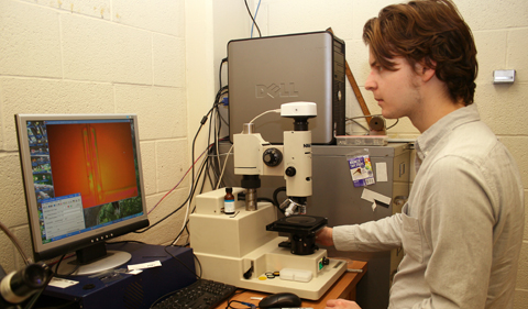
The main goal of my 2015 internship in Physics & Astronomy was to optimize the process of photolithography. I worked with Dr. Eric Stinaff, who had been developing the process with students. With his help, I managed to find a process that developed samples very consistently.
Photolithography involves building a flat circuit on a small substrate, often silicon or silicon dioxide. Using a spin coater, a gelatin-like photoresist is uniformly deposited onto the surface of a clean substrate. Following the application of a film of photoresist, the substrate is placed under a mask that blocks part of the sample while a bright LED lamp shines over the mask and sample.
These blocked regions of the resist are not exposed to the UV light initially, and the resist comes off during the development of the photoresist after the image reversal bake and flood expose. After this, a thin film of metal can be sputtered onto the sample. Once this process is complete and the excess metal is stripped off, a metal pattern is left on the silicon wafer.
One experiment I was able to conduct was observing the electric field between the two adjacent probes using quantum dots. I will be conducting further experiments with quantum dots using similar devices in the future.
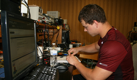
Throughout the summer, I learned basic lab protocol, as well as how to operate a few different machines, such as the RF and DC plasma cleansers in Clippinger. I managed to develop a consistent and effective protocol for the photolithographic facilities the department has, and was able to assist other researchers with any problems they had in their own similar processes.
I hope that my results can be easily taught to other researchers, providing the department with a method for creating their own nanoscale devices.
Miles Lindquist – 2015 Intern with Dr. Eric Stinaff – junior at Ohio University – Honors Tutorial College – astrophysics major


Comments